



Non-volatile memory for automotive, industrial, communications and IoT designs.
NOR flash, NAND flash, e.MMC, secure flash and ROM, offered across standard voltages, densities and package options, with design support from our engineering team.
NOR flash
| Family | Vcc | Density | Highlights |
|---|---|---|---|
| Octal I/O NOR flash | 1.8 V · 3 V | 64 Mb – 2 Gb | Octal I/O with DTR at up to 200 MHz, extending serial NOR throughput for fast boot and execute-in-place. |
| Serial NOR flash | 1.8 V · 2.5 V · 3 V | 512 Kb – 2 Gb | Multi I/O, DTR, dual quad, default lock protection, security and RPMC options in low pin count, small form factor packages. |
| Wide-range Vcc flash | 1.65 – 3.6 V | 512 Kb – 64 Mb | Standard serial NOR interface with ultra-low power consumption for battery-powered designs. |
| 1.2 V serial NOR flash | 1.2 V | — | Reduced supply voltage for health monitoring, Bluetooth, wearables and mobile internet devices. |
| Parallel NOR flash | 1.8 V · 3 V · 5 V | 2 Mb – 1 Gb | Uniform and boot sector, page mode, AD-mux and burst mode, read-while-write and security options. |
NAND, managed and specialty memory
| Family | Interface | Highlights |
|---|---|---|
| SLC NAND flash | Parallel | Single-level cell NAND for code and data storage where endurance and reliability matter. |
| Serial NAND flash | SPI | NAND density behind a low pin count serial interface. |
| e.MMC | e.MMC | Managed NAND with an integrated controller for embedded storage. |
| Secure flash | Serial | Authenticated, protected storage for secure boot, keys and firmware in connected devices. |
| ROM | Serial · Parallel | Mask ROM for fixed code and content at volume. |
Package options
Memory qualified for the conditions your product runs in.
Automotive
Industrial
Communications
Extended temperature
Known good die
Wafer level chip scale package
Security
IoT
Process technology for the fab we are building in India.
Accord Prime is in the process of setting up a semiconductor fab in India. Our process technology roadmap covers 6-inch and 8-inch wafer manufacturing for IC design companies and IDMs.
- 01Flat cell, OTP and embedded NVM
For MCUs and speech ICs.
- 02High-voltage CMOS
For LCD/LED driver ICs and power management ICs.
- 03Ultra-high-voltage process
For lighting applications.
- 04CD and BCD
CMOS-DMOS and Bipolar-CMOS-DMOS technology development, alongside analog, mixed-signal and MEMS processes.
- 05Customised technology
Cost-effective process options tailored to a customer's product.
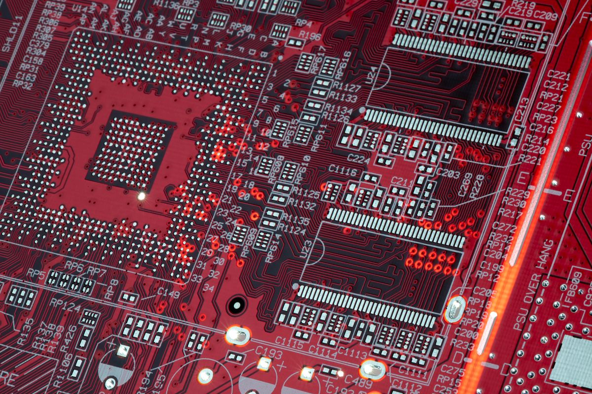 Reference platforms & reusable IP
Reusable platforms that shorten the path from design to deployment.
Alongside custom engagements, our teams maintain a set of reference platforms and tools that our customers and our own programs draw on directly.
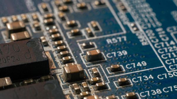
Evaluation & Reference Boards
Characterization-ready evaluation boards built to validate new silicon against datasheet specifications across voltage, temperature, and process corners.
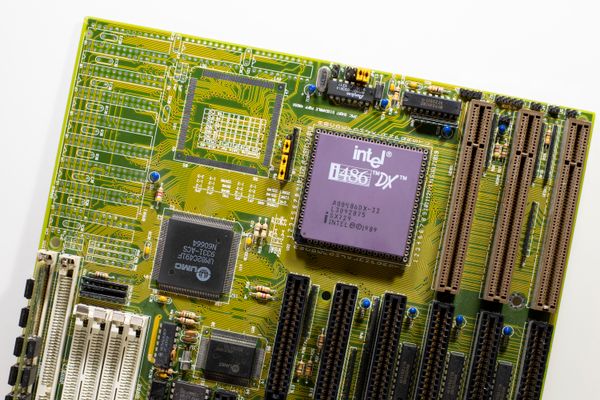
ATE Load Boards & Burn-In Boards
Test-side hardware, including ATE PCBs and burn-in boards, engineered alongside product boards to support production test and reliability screening.
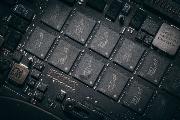
Reusable IP & Test Pattern Libraries
DFT and ATPG pattern sets, scan and MBIST building blocks, and verification collateral reused across programs to reduce design cycle time.
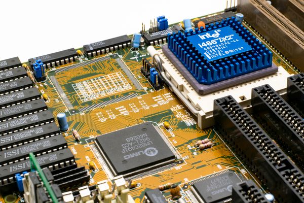
Test & Monitoring Automation Tools
Lightweight automation and data-capture tooling used internally to speed up characterization, yield analysis, and production test reporting.